Repurposing a PLC clone for use with Arduino
It is fairly common to find in online shopping pages, advertising like this: “Industrial control board compatible with FX1N, FX2N, FX3U and programmable with GX software”. The price is attractive, however, the documentation is non-existent, and there is no mention of how to program it with other tools like Arduino in other operating systems different from Windows. This article will introduce a few key concepts to help solve this problem.
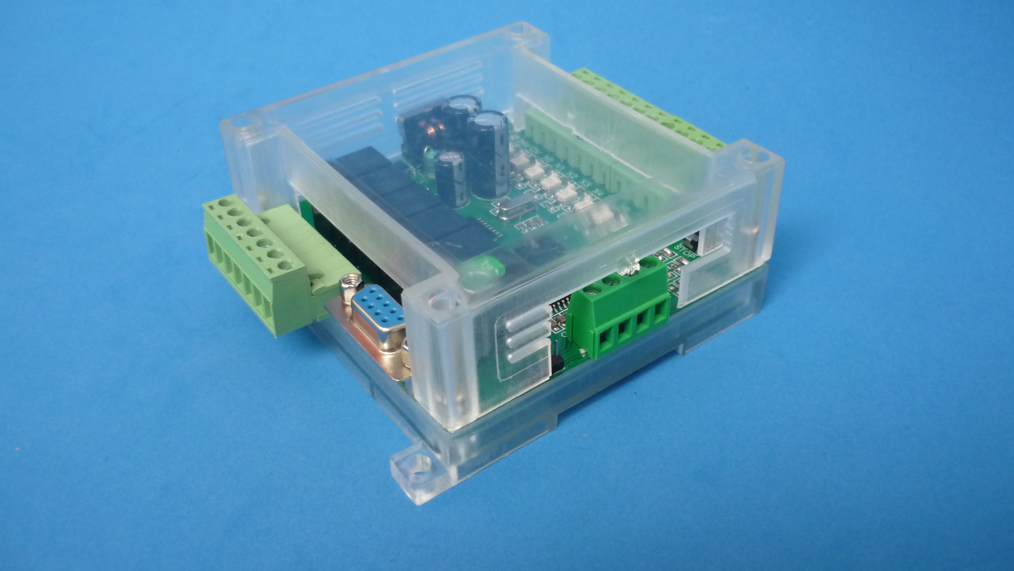
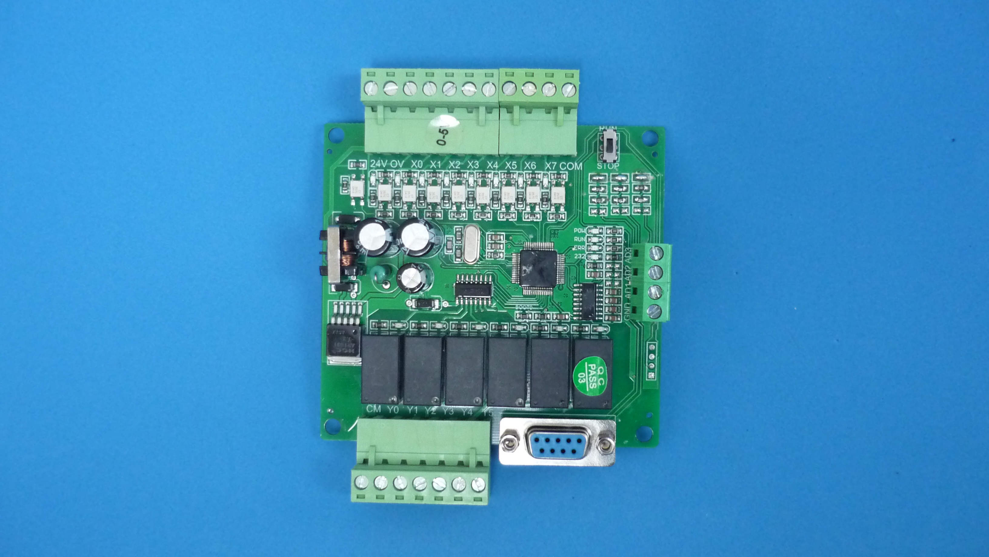
Key component: Industrial control board compatible with FX1N
Attack of the clones
These boards mention compatibility with GX software, which is manufactured by a Japanese company that makes PLC and also cars. At first sight, the compatibility is not official, as no trademark is printed. Their origin is unknown, maybe they were simplified copies based on original schematics and source code, or somehow the native binary format of the PLC was reverse engineered and an interpreter was built and runs in the microcontroller translating the code. Most of the cards are based on STM32 microcontrollers, and according to some articles and videos, the original programming software actually recognizes them as an original PLC!
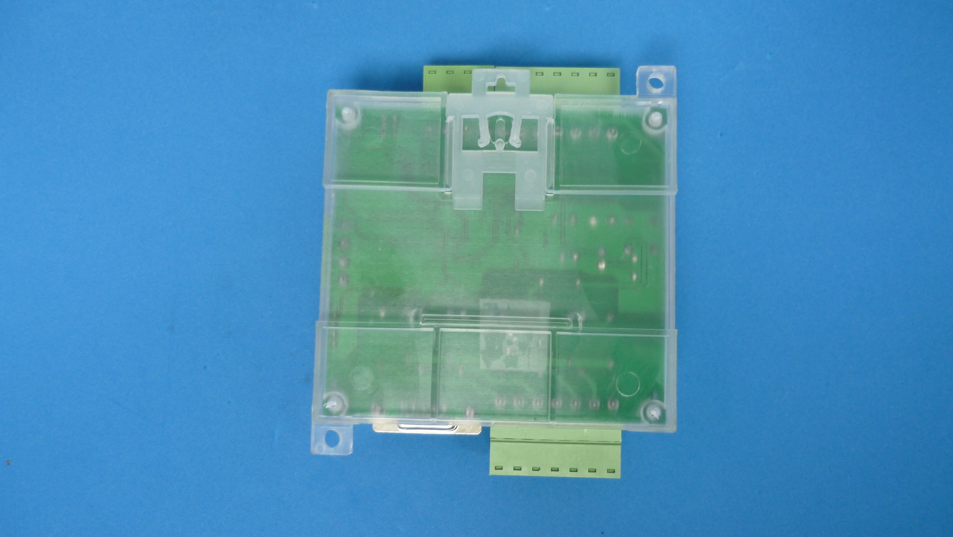
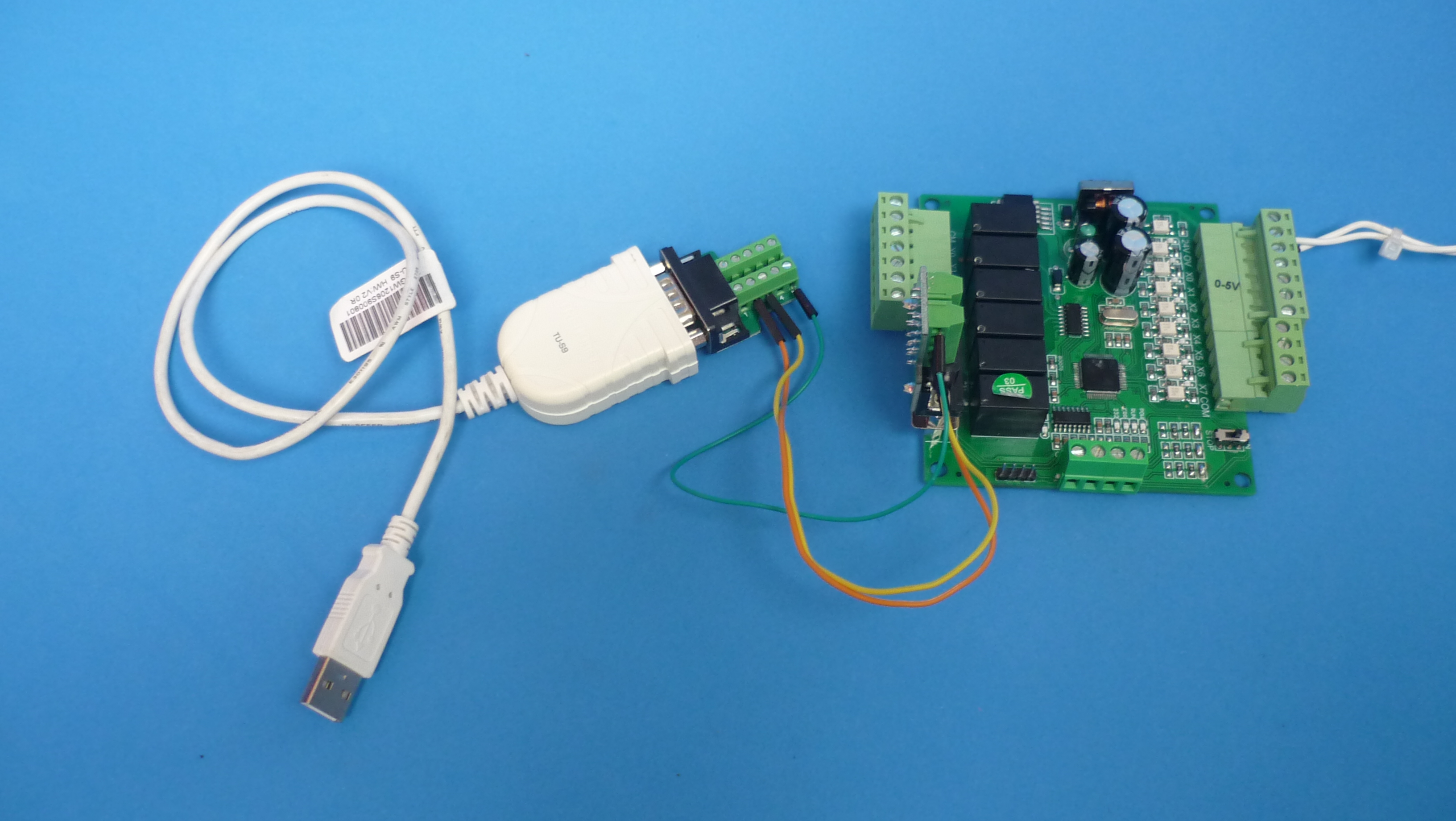
Due to their low cost (around $25 USD), and for their relay isolated outputs, optically isolated inputs, RS232 serial port and regulated power supply, are great candidates for small projects as long as they can be programmed with a free multi-platform tool like Arduino or STM suite. In addition, a schematic diagram is needed to find out which I/O of the microcontroller goes to which peripheral in the board!
Bill of materials
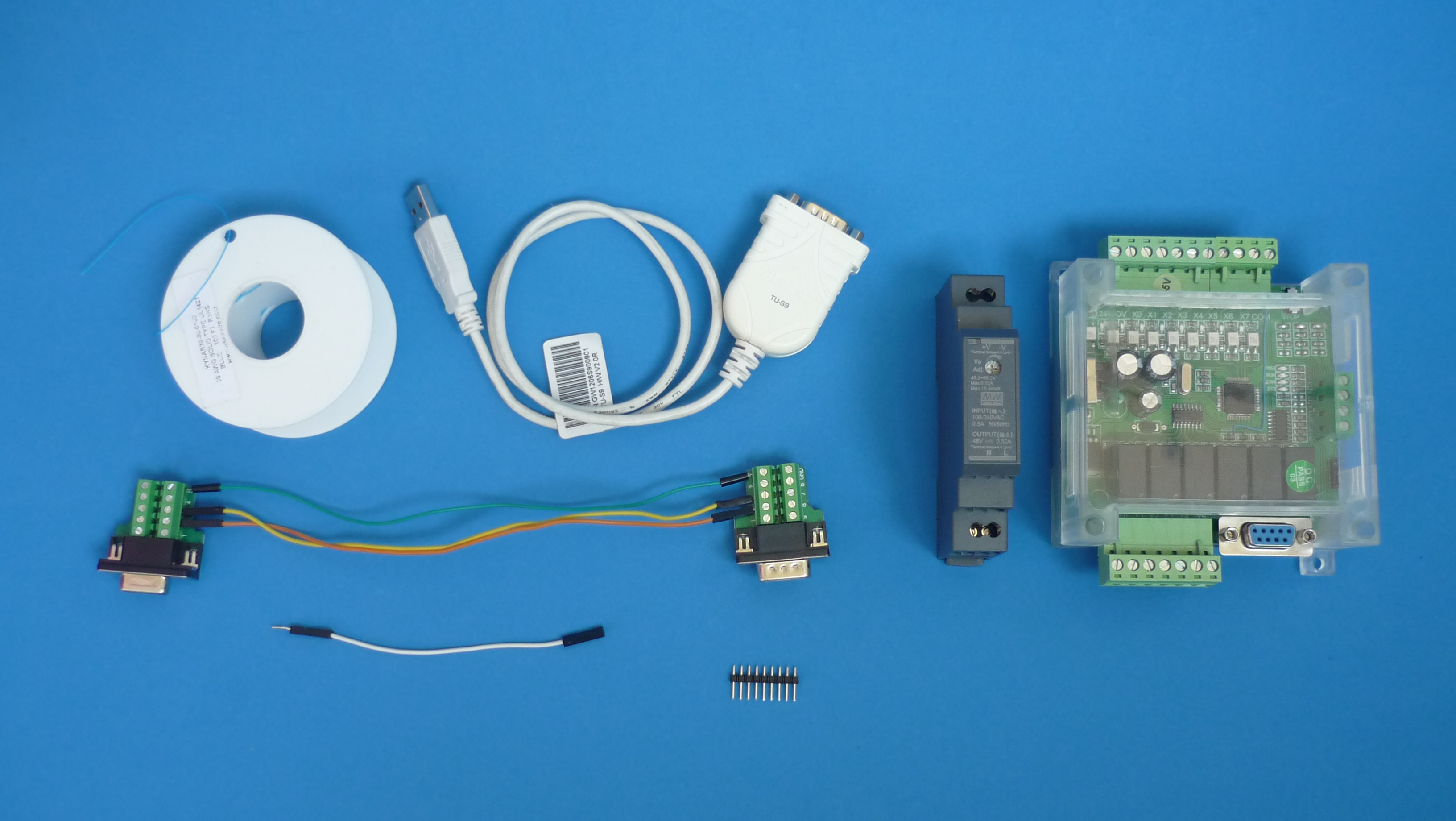
| Component | Buy link | Datasheet |
|---|---|---|
| Industrial control board compatible with FX1N | buy it | industrial-control-board-fx1n.pdf |
| 24 V 15 W DIN rail mount power supply | buy it | 24v-din-rail-power-supply.pdf |
| USB to RS232 converter | buy it | usb-rs232-converter.pdf |
| DB9 solderless terminal connector | buy it | db9-solderless-terminal-connector.pdf |
| 30 AWG UL1423 type PVDF wire | buy it | UL1423.pdf |
| Dupont cable jumper | buy it | dupont-jumper-cables.pdf |
| Single line male header 2.54mm | buy it | FHA3-S1XX.pdf |
| Pinout for industrial control boards | repository |
|---|---|
| Industrial control boards based on STM32 | stm32-industrial-control-boards |
| Optional component | Buy link | Datasheet |
|---|---|---|
| Magnifying double eye for jewelry | buy it | magnifying-double-eye.pdf |
| USB digital microscope camera | buy it | microscope-camera-digital-usb.pdf |
| Digital multimeter powered by AA batteries | buy it | digital-multimeter-powered-aa-batteries-ut139c.pdf |
Reprograming
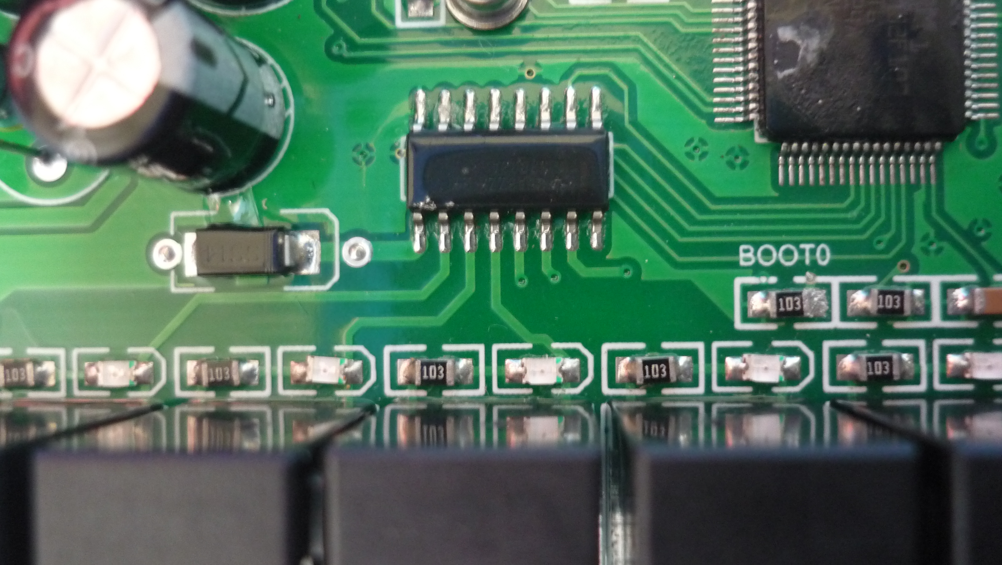
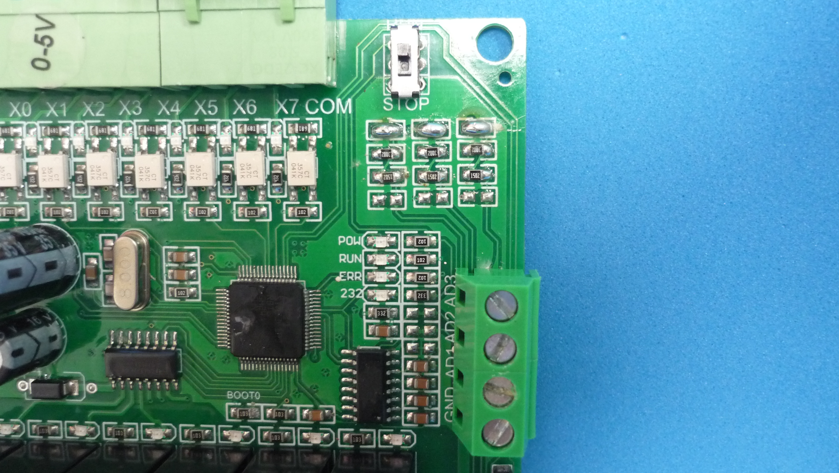
The aforementioned board, sports a STM32F103 microcontroller, so instinctively a footprint for a SWD programming header should be looked for.
After following the tracks of this header, one pin was found connected to 3.3 V, another one to GND, but the other two pins were not connected to SWD pins on the microcontroller but to PC10 and PC11 pins. Starting the search from the microcontroller, there are no tracks from SWD or USB pins, so the only alternative available for reprogramming is through UART1 using the bootloader stored in ROM
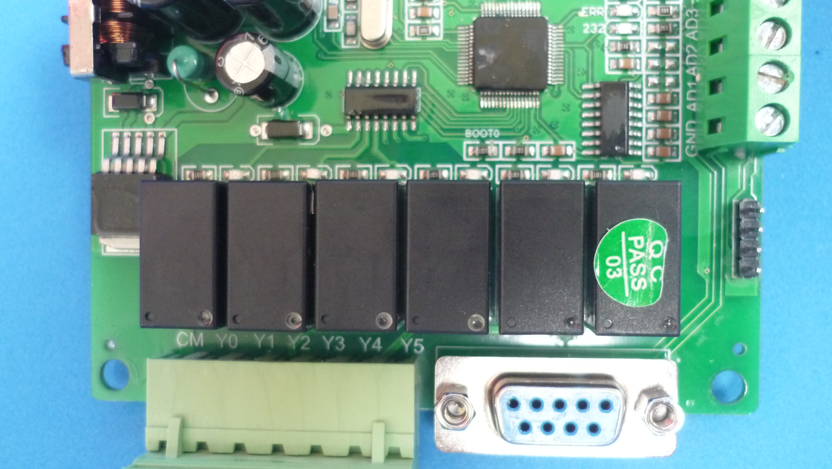
Following the tracks leaving from the DB9 connector, they end in an unmarked chip, however, due to the nearby capacitors it is probably a MAX232 or equivalent. Following the tracks leaving from this chip they end in PA9 and PA10 pins of the microcontroller which are the UART1 pins.
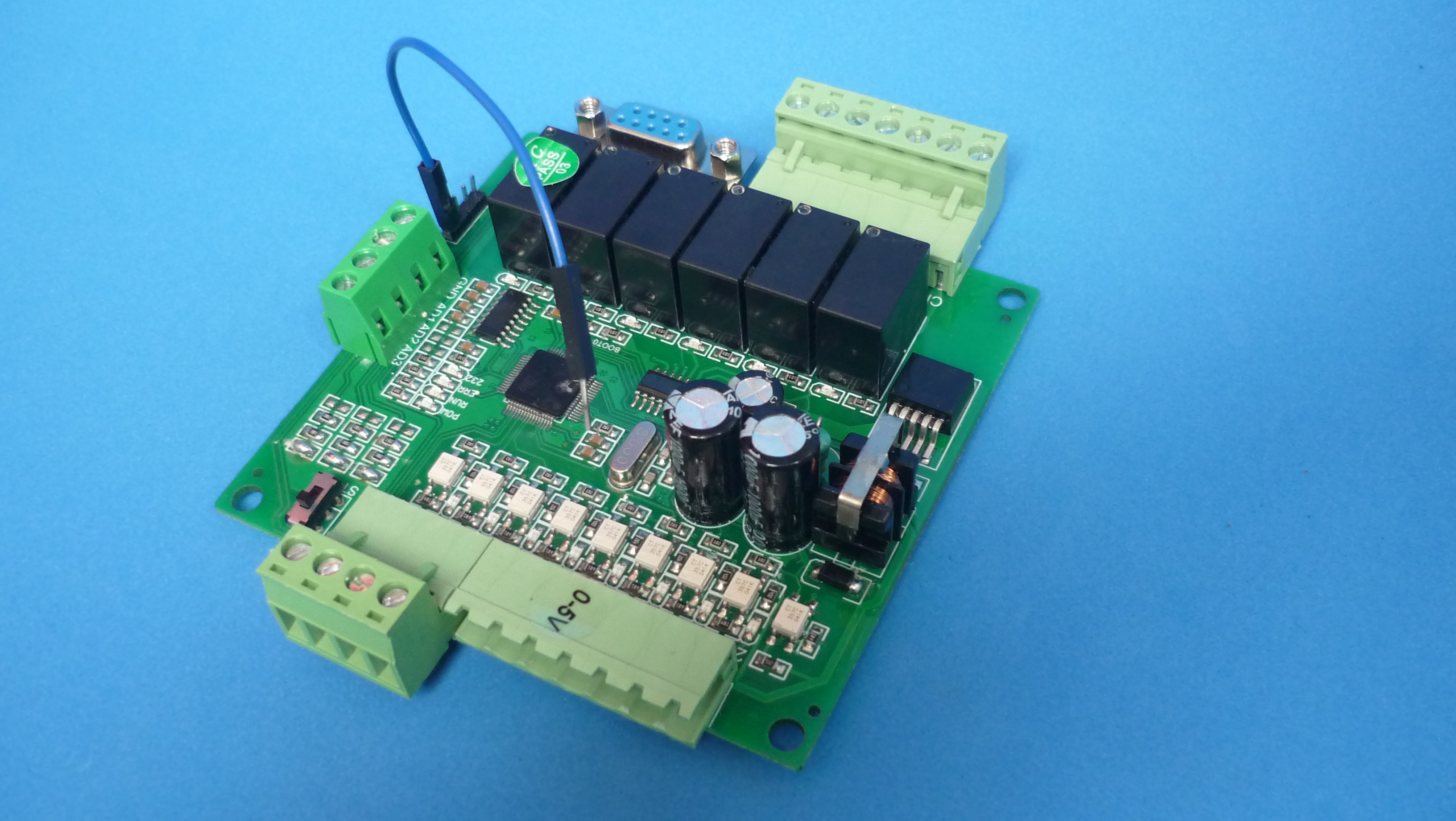
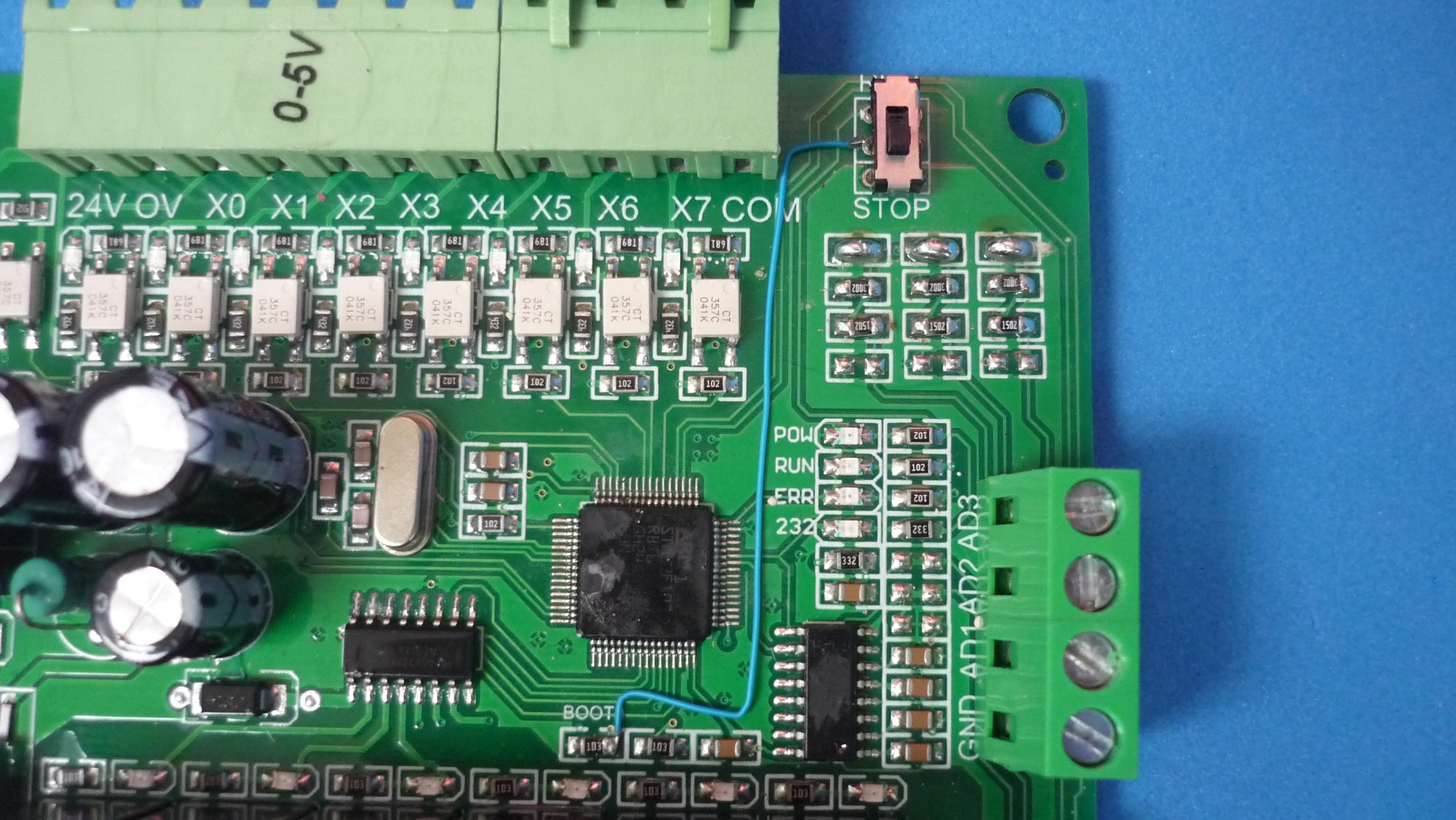
Luckily in this board, the resistor which is connected to the BOOT0 pin is clearly marked on the silkscreen. To start in bootloader mode, a male header was soldered to the 3.3 V pad, and using a Dupont wire jumper, a temporary connection between BOOT0 and 3.3 V is made while the board is powered up
Once the bootloader was running, STM32CubeProg was launched and communication with the microcontroller was verified. The chip was in read protect mode, so no way to backup the firmware to reverse the board to its original state. All FLASH memory has been erased.
Using Arduino IDE, it was proceeded to the installation STM32duino core and to make a small test application that sends data through the serial port to the PC. The app was downloaded and the incoming data verified. Now the adventure starts!
Identifying I/O pins
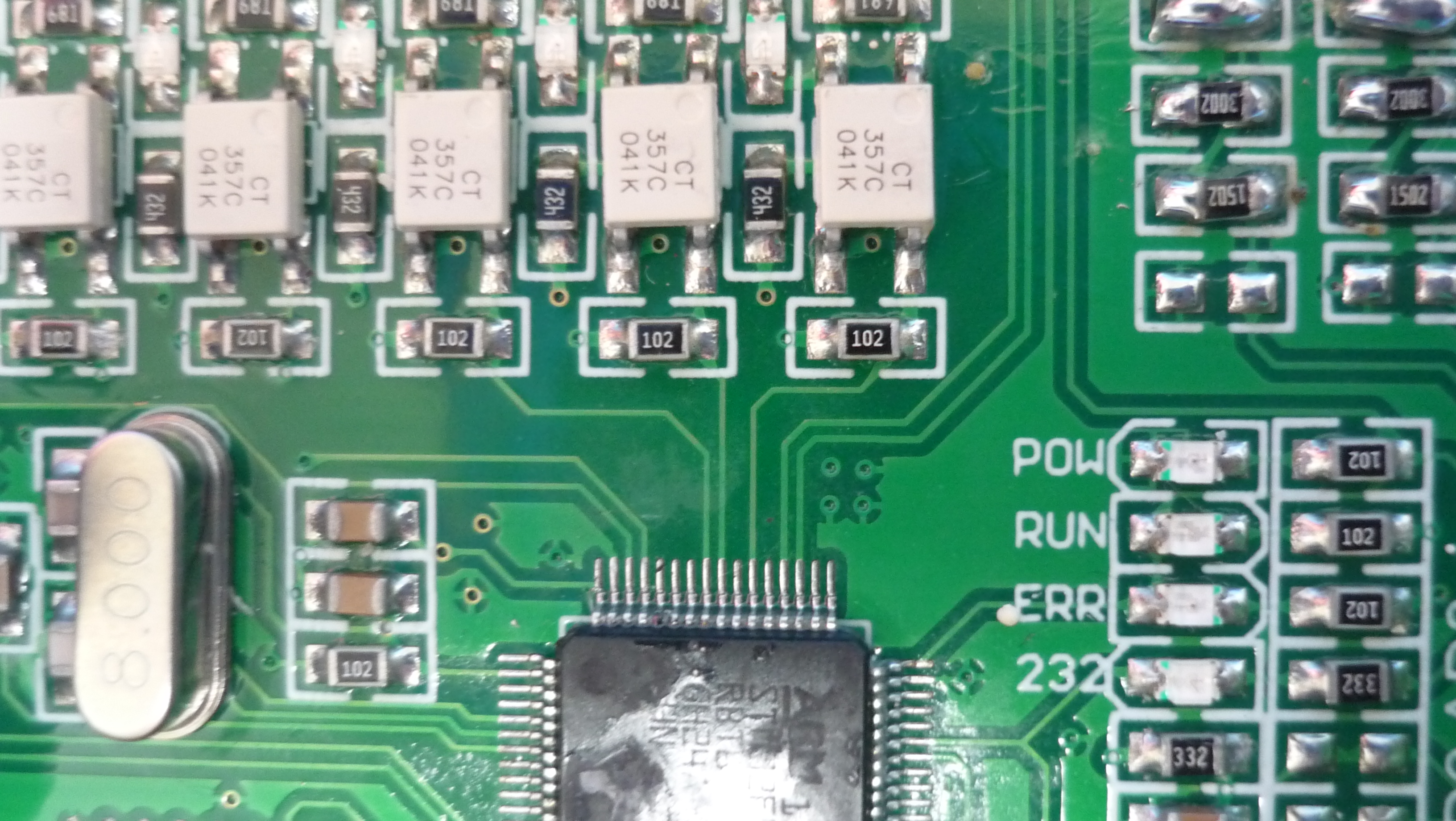
Because of the lack of a schematic diagram, or marks in the silkscreen showing which microcontroller I/O pins goes to which peripheral, this work must be done manually, with a lot of patience to follow the tracks. Fortunately the board has only 2 layers, so it is possible to start with only a double-eye magnifier for jewelry and a multimeter.
LED and switch
The board has two LED indicators, one labeled as RUN an the other labeled as ERR. Additionally, there is a switch that was used by the old PLC firmware to stop program execution. Due to these peripherals have a few elements between them and the microcontroller, they are very easy to start with.
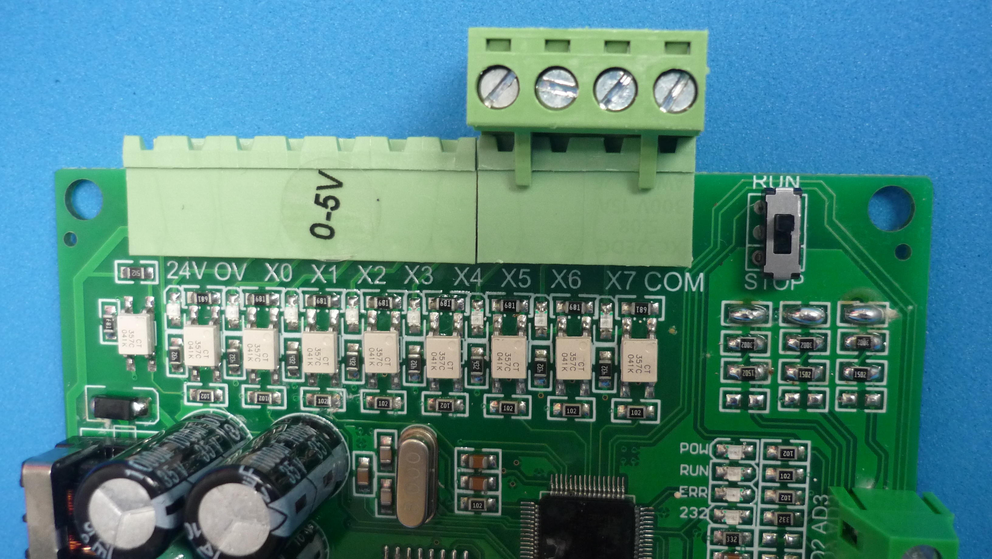
The pins were found mapped as follows:
| ELEMENT | PIN |
|---|---|
| LED RUN | PB12 |
| LED ERR | PB13 |
| RUN/STOP SWITCH | PC9 |
Digital inputs
Digital inputs were relatively easy to find, because the tracks leaving the optocuplers went directly to the microcontroller. Only a few ones were tricky because they jumped to the opposite layer or traveled under a big component.
The pins were found mapped as follows:
| ELEMENT | PIN |
|---|---|
| X0 | PA0 |
| X1 | PA1 |
| X2 | PB9 |
| X3 | PA6 |
| X4 | PA7 |
| X5 | PB5 |
| X6 | PB4 |
| X7 | PD2 |
Digital outputs
The digital outputs took the most effort, because the tracks went first to an UL2003 chip, and from there to each relay, traveling under components or jumping to the opposite layer. Multimeter was crucial to follow the tracks.
The pins were found mapped as follows:
| ELEMENT | PIN |
|---|---|
| Y0 | PB8 |
| Y1 | PB1 |
| Y2 | PB10 |
| Y3 | PB0 |
| Y4 | PC5 |
| Y5 | PC4 |
Analog inputs
The analog inputs were relatively easy to find, because they are only 3 and they are connected only to a voltage resistor divider (15 K/30 K) between them and the microcontroller.
The pins were found mapped as follows:
| ELEMENT | PIN |
|---|---|
| AD1 | PC1 |
| AD2 | PC2 |
| AD3 | PC0 |
Final touches
At this point, all peripherals are mapped to the microcontroller I/O pins, however, whenever the board needs to be reprogrammed, BOOT0 needs to be set to 3.3 V using a temporal wire jumper, which implies opening the enclosure. A quick fix will be to connect a wire from the BOOT0 pin to the RUN/STOP switch used by the old PLC firmware, in this way the ROM bootloader could be initiated externally without opening the case for reprogramming
Summarizing
At this stage, you have a low cost board with enough peripherals for small experiments without requiring additional hardware and can be programmed using Arduino IDE or STM suite. To replicate this experiment with a different board (as long as the CPU has been identified) follow the steps below:
- Look for SWD header footprint on the PCB (4 pads) and follow the tracks to the microcontroller to make sure the pins are the right ones.
- If the previous step fails, follow the tracks from the UART1 pins of the microcontroller and add the additional hardware (level converter, connectors) for PC communication
- Look for BOOT0 pin, it is usually connected to the ground through a resistor, it will serve as a “test point”
- Using STM32CubeProg erase the microcontroller FLASH memory, If UART1 was used as a connection means, the ROM bootloader must be launched, setting BOOT0 to 3.3 V while powering on the board.
- Using the Arduino IDE or the STM suite, make a little test application, which sends characters to the serial port, to know if the board could be programmed
- Follow the tracks from the peripherals to the microcontroller, to make the I/O pin mapping
- Make a wire connection from BOOT0 to the RUN/STOP switch to easily program the board
Possible improvements
Create a skeleton application as a boiler plate for each program for the board, this application should have some kind of mechanism that checks the condition of the RUN/STOP switch to decide whether to go to ROM bootloader or start executing the program stored in the FLASH, This eliminates the need for an electrical connection between BOOT0 and the switch.
Another option, if a skeleton app is not desired, is to make a bootloader stored in the FLASH that uses UART1 for communication, similar to the one stored in ROM, but this one checks the condition of the RUN/STOP switch to decide whether to download a new program or executing the program stored in the FLASH